- 您现在的位置:买卖IC网 > Sheet目录319 > COP8SG-EPU (National Semiconductor)BOARD PROTOTYPE/TARGET COP8
�� �
�
�Timers�
�(Continued)�
�The� underflows� can� be� programmed� to� toggle� the� TxA� output�
�pin.� The� underflows� can� also� be� programmed� to� generate� in-�
�terrupts.�
�Underflows� from� the� timer� are� alternately� latched� into� two�
�pending� flags,� TxPNDA� and� TxPNDB.� The� user� must� reset�
�these� pending� flags� under� software� control.� Two� control� en-�
�able� flags,� TxENA� and� TxENB,� allow� the� interrupts� from� the�
�timer� underflow� to� be� enabled� or� disabled.� Setting� the� timer�
�enable� flag� TxENA� will� cause� an� interrupt� when� a� timer� un-�
�derflow� causes� the� RxA� register� to� be� reloaded� into� the� timer.�
�Setting� the� timer� enable� flag� TxENB� will� cause� an� interrupt�
�when� a� timer� underflow� causes� the� RxB� register� to� be� re-�
�loaded� into� the� timer.� Resetting� the� timer� enable� flags� will�
�disable� the� associated� interrupts.�
�Either� or� both� of� the� timer� underflow� interrupts� may� be� en-�
�abled.� This� gives� the� user� the� flexibility� of� interrupting� once�
�per� PWM� period� on� either� the� rising� or� falling� edge� of� the�
�PWM� output.� Alternatively,� the� user� may� choose� to� interrupt�
�on� both� edges� of� the� PWM� output.�
�DS012829-10�
�FIGURE� 8.� Timer� in� PWM� Mode�
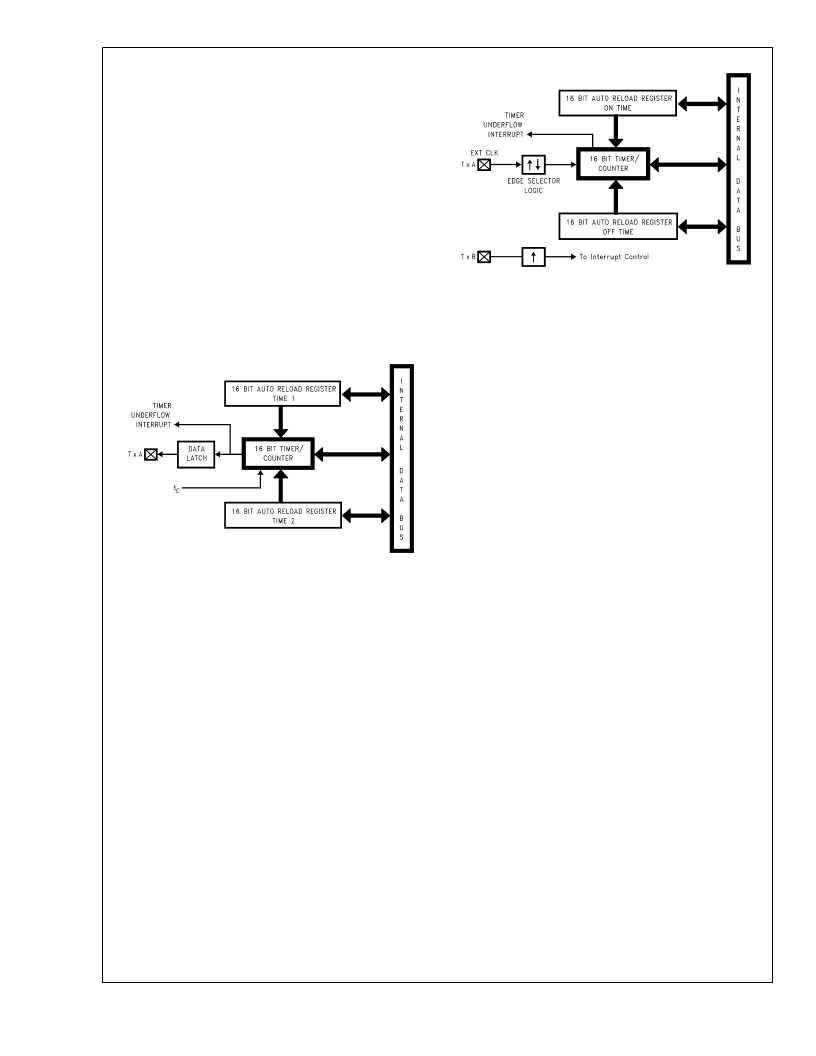
�Mode� 2.� External� Event� Counter� Mode�
�This� mode� is� quite� similar� to� the� processor� independent�
�PWM� mode� described� above.� The� main� difference� is� that� the�
�timer,� Tx,� is� clocked� by� the� input� signal� from� the� TxA� pin.� The�
�Tx� timer� control� bits,� TxC3,� TxC2� and� TxC1� allow� the� timer� to�
�be� clocked� either� on� a� positive� or� negative� edge� from� the�
�TxA� pin.� Underflows� from� the� timer� are� latched� into� the� TxP-�
�NDA� pending� flag.� Setting� the� TxENA� control� flag� will� cause�
�an� interrupt� when� the� timer� underflows.�
�In� this� mode� the� input� pin� TxB� can� be� used� as� an� indepen-�
�dent� positive� edge� sensitive� interrupt� input� if� the� TxENB� con-�
�trol� flag� is� set.� The� occurrence� of� a� positive� edge� on� the� TxB�
�input� pin� is� latched� into� the� TxPNDB� flag.�
�Figure� 9� shows� a� block� diagram� of� the� timer� in� External�
�Event� Counter� mode.�
�Note:� The� PWM� output� is� not� available� in� this� mode� since� the� TxA� pin� is� being�
�used� as� the� counter� input� clock.�
�www.national.com�
�20�
�DS012829-11�
�FIGURE� 9.� Timer� in� External� Event� Counter� Mode�
�Mode� 3.� Input� Capture� Mode�
�The� device� can� precisely� measure� external� frequencies� or�
�time� external� events� by� placing� the� timer� block,� Tx,� in� the� in-�
�put� capture� mode.�
�In� this� mode,� the� timer� Tx� is� constantly� running� at� the� fixed� t� c�
�rate.� The� two� registers,� RxA� and� RxB,� act� as� capture� regis-�
�ters.� Each� register� acts� in� conjunction� with� a� pin.� The� register�
�RxA� acts� in� conjunction� with� the� TxA� pin� and� the� register� RxB�
�acts� in� conjunction� with� the� TxB� pin.�
�The� timer� value� gets� copied� over� into� the� register� when� a�
�trigger� event� occurs� on� its� corresponding� pin.� Control� bits,�
�TxC3,� TxC2� and� TxC1,� allow� the� trigger� events� to� be� speci-�
�fied� either� as� a� positive� or� a� negative� edge.� The� trigger� con-�
�dition� for� each� input� pin� can� be� specified� independently.�
�The� trigger� conditions� can� also� be� programmed� to� generate�
�interrupts.� The� occurrence� of� the� specified� trigger� condition�
�on� the� TxA� and� TxB� pins� will� be� respectively� latched� into� the�
�pending� flags,� TxPNDA� and� TxPNDB.� The� control� flag� Tx-�
�ENA� allows� the� interrupt� on� TxA� to� be� either� enabled� or� dis-�
�abled.� Setting� the� TxENA� flag� enables� interrupts� to� be� gener-�
�ated� when� the� selected� trigger� condition� occurs� on� the� TxA�
�pin.� Similarly,� the� flag� TxENB� controls� the� interrupts� from� the�
�TxB� pin.�
�Underflows� from� the� timer� can� also� be� programmed� to� gen-�
�erate� interrupts.� Underflows� are� latched� into� the� timer� TxC0�
�pending� flag� (the� TxC0� control� bit� serves� as� the� timer� under-�
�flow� interrupt� pending� flag� in� the� Input� Capture� mode).� Con-�
�sequently,� the� TxC0� control� bit� should� be� reset� when� enter-�
�ing� the� Input� Capture� mode.� The� timer� underflow� interrupt� is�
�enabled� with� the� TxENA� control� flag.� When� a� TxA� interrupt�
�occurs� in� the� Input� Capture� mode,� the� user� must� check� both�
�the� TxPNDA� and� TxC0� pending� flags� in� order� to� determine�
�whether� a� TxA� input� capture� or� a� timer� underflow� (or� both)�
�caused� the� interrupt.�
�Figure� 10� shows� a� block� diagram� of� the� timer� in� Input� Cap-�
�ture� mode.�
�发布紧急采购,3分钟左右您将得到回复。
相关PDF资料
CORE1553-DEV-KIT
KIT DEVELOPMENT FOR IP CORE1553
CP131-AG
LNR PWR SUP 5V 8A, +/-12V 1.7A
CPC1590P
MOSFET GATE DVR ISO 8-FLATPACK
CPC5002G
ISOLAT DGTL 3.75KVRMS 2CH 8-DIP
CPCI-D-3U-300C
PWR SUPLY DC/DC CPCI 300W 3UX8HP
CPD250-4530G
PWR SUP 250W 3.3/5/12/-12V QUAD
CS4161YN8
IC DRIVER H-BRDG DUAL 85MA 8DIP
CS5461A-ISZ
IC ENERGY METERING 1PHASE 24SSOP
相关代理商/技术参数
COP8SGR728M7
功能描述:8位微控制器 -MCU RoHS:否 制造商:Silicon Labs 核心:8051 处理器系列:C8051F39x 数据总线宽度:8 bit 最大时钟频率:50 MHz 程序存储器大小:16 KB 数据 RAM 大小:1 KB 片上 ADC:Yes 工作电源电压:1.8 V to 3.6 V 工作温度范围:- 40 C to + 105 C 封装 / 箱体:QFN-20 安装风格:SMD/SMT
COP8SGR728M7/NOPB
功能描述:8位微控制器 -MCU RoHS:否 制造商:Silicon Labs 核心:8051 处理器系列:C8051F39x 数据总线宽度:8 bit 最大时钟频率:50 MHz 程序存储器大小:16 KB 数据 RAM 大小:1 KB 片上 ADC:Yes 工作电源电压:1.8 V to 3.6 V 工作温度范围:- 40 C to + 105 C 封装 / 箱体:QFN-20 安装风格:SMD/SMT
COP8SGR728M8
功能描述:8位微控制器 -MCU RoHS:否 制造商:Silicon Labs 核心:8051 处理器系列:C8051F39x 数据总线宽度:8 bit 最大时钟频率:50 MHz 程序存储器大小:16 KB 数据 RAM 大小:1 KB 片上 ADC:Yes 工作电源电压:1.8 V to 3.6 V 工作温度范围:- 40 C to + 105 C 封装 / 箱体:QFN-20 安装风格:SMD/SMT
COP8SGR728M8/NOPB
功能描述:8位微控制器 -MCU RoHS:否 制造商:Silicon Labs 核心:8051 处理器系列:C8051F39x 数据总线宽度:8 bit 最大时钟频率:50 MHz 程序存储器大小:16 KB 数据 RAM 大小:1 KB 片上 ADC:Yes 工作电源电压:1.8 V to 3.6 V 工作温度范围:- 40 C to + 105 C 封装 / 箱体:QFN-20 安装风格:SMD/SMT
COP8SGR728N8
功能描述:8位微控制器 -MCU RoHS:否 制造商:Silicon Labs 核心:8051 处理器系列:C8051F39x 数据总线宽度:8 bit 最大时钟频率:50 MHz 程序存储器大小:16 KB 数据 RAM 大小:1 KB 片上 ADC:Yes 工作电源电压:1.8 V to 3.6 V 工作温度范围:- 40 C to + 105 C 封装 / 箱体:QFN-20 安装风格:SMD/SMT
COP8SGR728N8/NOPB
功能描述:8位微控制器 -MCU RoHS:否 制造商:Silicon Labs 核心:8051 处理器系列:C8051F39x 数据总线宽度:8 bit 最大时钟频率:50 MHz 程序存储器大小:16 KB 数据 RAM 大小:1 KB 片上 ADC:Yes 工作电源电压:1.8 V to 3.6 V 工作温度范围:- 40 C to + 105 C 封装 / 箱体:QFN-20 安装风格:SMD/SMT
COP8SGR740N8
功能描述:IC MCU 8BIT CMOS OTP 40DIP RoHS:否 类别:集成电路 (IC) >> 嵌入式 - 微控制器, 系列:COP8™ 8SG 其它有关文件:STM32F101T8 View All Specifications 特色产品:STM32 32-bit Cortex MCUs 标准包装:490 系列:STM32 F1 核心处理器:ARM? Cortex?-M3 芯体尺寸:32-位 速度:36MHz 连通性:I²C,IrDA,LIN,SPI,UART/USART 外围设备:DMA,PDR,POR,PVD,PWM,温度传感器,WDT 输入/输出数:26 程序存储器容量:64KB(64K x 8) 程序存储器类型:闪存 EEPROM 大小:- RAM 容量:10K x 8 电压 - 电源 (Vcc/Vdd):2 V ~ 3.6 V 数据转换器:A/D 10x12b 振荡器型:内部 工作温度:-40°C ~ 85°C 封装/外壳:36-VFQFN,36-VFQFPN 包装:托盘 配用:497-10030-ND - STARTER KIT FOR STM32497-8853-ND - BOARD DEMO STM32 UNIV USB-UUSCIKSDKSTM32-PL-ND - KIT IAR KICKSTART STM32 CORTEXM3497-8512-ND - KIT STARTER FOR STM32F10XE MCU497-8505-ND - KIT STARTER FOR STM32F10XE MCU497-8304-ND - KIT STM32 MOTOR DRIVER BLDC497-6438-ND - BOARD EVALUTION FOR STM32 512K497-6289-ND - KIT PERFORMANCE STICK FOR STM32MCBSTM32UME-ND - BOARD EVAL MCBSTM32 + ULINK-MEMCBSTM32U-ND - BOARD EVAL MCBSTM32 + ULINK2更多... 其它名称:497-9032STM32F101T8U6-ND
COP8SGR740N8/NOPB
制造商:Texas Instruments 功能描述: